The future of the semiconductor industry depends on advanced materials for semiconductor and advanced wafer fabrication materials that provide the essential foundation for innovation, sustainability, and efficiency. Advanced materials and wafer fabrication solutions are at the forefront of this development, enabling the creation of high-performance, reliable, and sustainable semiconductor devices that power the modern world. The advanced materials for semiconductor market reached an estimated USD 6.42 billion in 2024 and is projected to grow to USD 13.95 billion by 2035, registering a CAGR of 7.32%. At the foundation of the future of electronics are advanced materials for semiconductor and advanced wafer fabrication materials, which together are building the next generation of semiconductor devices.
The Foundation: Advanced Materials for Semiconductor
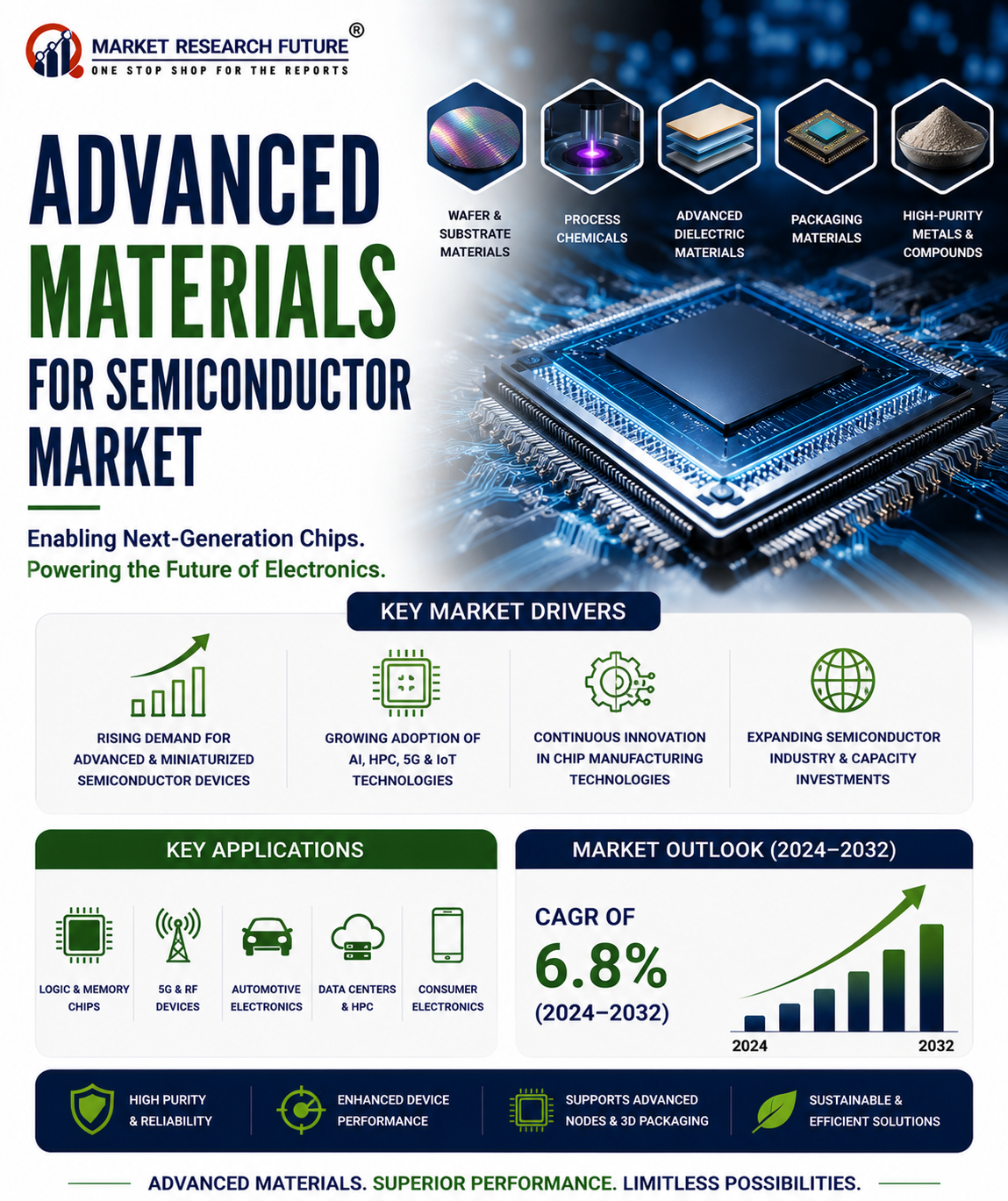
Advanced materials for semiconductor provide the essential materials and compounds required for fabricating integrated circuits, including silicon wafers, high-purity chemicals, specialty gases, and advanced packaging materials. These materials are critical for achieving the performance, density, and reliability demanded by modern electronic devices. Silicon holds the largest share attributed to its established presence and reliability in semiconductor applications, while advanced materials such as gallium nitride (GaN) and silicon carbide (SiC) are rapidly gaining traction due to their superior efficiency in high-performance applications, particularly in power electronics and electric vehicles. The enduring demand for traditional silicon-based devices is relentless, predominantly driven by the consumer electronics sector, while advanced materials are essential for emerging applications in power electronics, 5G communications, and electric vehicles.
The foundation of advanced materials for semiconductor is built on continuous innovation in materials science, purification technology, and quality control. Manufacturers are developing materials with improved properties, higher purity, and better consistency to meet the demands of advanced semiconductor applications. The focus on sustainability is driving the development of eco-friendly materials that minimize environmental impact while maintaining performance. The integration of advanced materials is enabling the continued scaling of semiconductor devices, allowing for more functionality in smaller form factors and supporting emerging applications such as artificial intelligence and quantum computing.
The Structure: Advanced Wafer Fabrication Materials
Advanced wafer fabrication materials encompass the specialized substances and consumables used in the semiconductor manufacturing process, including photoresists, etchants, deposition precursors, CMP slurries, and high-purity gases. These materials are critical for achieving the precise patterning, layering, and planarization necessary for modern semiconductor devices. The semiconductor industry is increasingly adopting advanced materials such as high-k dielectrics, low-k interlayer dielectrics, and advanced photoresists to enable smaller, more complex device architectures. The development of advanced wafer fabrication materials is driven by the need for higher yields, lower defect rates, and improved device performance.
The structure of advanced wafer fabrication materials is characterized by the integration of multiple material types, each serving specific functions in the fabrication process. Silicon wafers remain the dominant substrate material due to their established presence and reliability. However, compound semiconductors such as gallium nitride and silicon carbide are gaining traction for high-performance applications. Photoresists and related materials enable precise patterning through advanced lithography techniques such as extreme ultraviolet (EUV) lithography. Deposition precursors and high-purity gases enable the growth of thin films with precise composition and thickness. The development of new materials with improved properties is expanding the application range, enabling new device architectures and applications.
Key Applications Driving Market Growth
Advanced materials for semiconductor and advanced wafer fabrication materials find applications across diverse sectors. In consumer electronics, these materials enable the production of smartphones, tablets, and laptops with increasing performance and decreasing size. The telecommunications industry relies on advanced materials for RF components and 5G infrastructure, which require superior signal integrity and performance. The automotive sector utilizes these materials for power devices and sensors in electric and autonomous vehicles, with SiC and GaN being pivotal in enhancing power electronics efficiency. The industrial sector employs advanced semiconductor materials for power electronics and control systems.
The consumer electronics segment holds the largest market share, driven by the escalating demand for electronics and the continuous push for miniaturization. The rise of electric vehicles (EVs) is a significant driver, with the EV market projected to grow substantially, creating opportunities for semiconductor manufacturers. Advanced materials such as silicon carbide and gallium nitride are pivotal in enhancing the efficiency and performance of power electronics in EVs, aligning with global sustainability goals.
Benefits of Advanced Semiconductor Materials
The benefits of advanced materials for semiconductor and advanced wafer fabrication materials extend across performance enhancement, miniaturization, and energy efficiency. Superior thermal and electrical properties enable higher performance and lower power consumption. Advanced materials enable the fabrication of smaller, more complex devices that pack more functionality into less space. Energy-efficient semiconductors contribute to reduced power consumption and longer battery life in portable devices. The adoption of these materials supports innovation and technological leadership, with the development of new materials with improved performance expanding the application range.
Future Trends and Opportunities
The future of advanced materials for semiconductor and advanced wafer fabrication materials is characterized by continued innovation in materials science, processing, and applications. Development of eco-friendly semiconductor materials for sustainable production is creating new opportunities. Investment in advanced packaging technologies is enhancing performance. Expansion into emerging markets with tailored semiconductor solutions is meeting regional needs. Focus on artificial intelligence and quantum computing applications is driving material innovation. Organizations that invest in innovative Advanced materials for semiconductor and Advanced Wafer Fabrication Materials will be well-positioned to lead the semiconductor industry, delivering the advanced, sustainable solutions demanded by next-generation electronic devices.